


4.1 The Electronic Band Structure of Silicon#
Notebook overview#
Why does silicon carry current the way it does, absorb the light it does, and sit at the heart of every chip? The answer is its band structure: the map of allowed electron energies as a function of crystal momentum. In a periodic solid the electronic states organise into bands, and the gap between the filled and empty ones decides whether a material is a metal, a semiconductor, or an insulator. Computing that map is the central task of electronic-structure theory.
This is the band-theory exercise of Lecture 5, and unlike the earlier volumes it is code-essential: density-functional theory cannot be reimplemented in a notebook, and the real skill is running the calculation and reading its output. So we work with the genuine article. We show the Quantum ESPRESSO input deck the course used for silicon, parse the real committed output of that density-functional calculation, plot the band structure along the high-symmetry path L–Γ–X, and read off the indirect gap. Then we confront the result with experiment, and meet the most famous systematic error in the field: the density-functional band-gap problem.
Provenance. This notebook develops Lecture 5 of the course (band theory of crystals), an exercise originally designed by Dr. Carlo Pignedoli, here redesigned and rephrased by the author. The band structure is parsed from the real output of the course’s Quantum ESPRESSO calculation of silicon (the committed
exercise-5/TASK_3/done/SI.xml), shown alongside the course’s own silicon SCF deck (scf.in). No part of the electronic structure is recomputed or invented; we read and analyse the actual DFT result. The full course credit is in the footer.
Reading a validation. Each exercise closes with a check against an independent fact: an electron count, the known position of silicon’s band extrema, the measured gap. A ✗ flags a mismatch to track down, not a verdict; a ✓ is strong evidence, not proof.
Theory in brief#
Bloch’s theorem and bands#
In a crystal the potential is periodic, \(V(\mathbf r+\mathbf R)=V(\mathbf r)\) for every lattice vector \(\mathbf R\). Bloch’s theorem then says the electronic eigenstates can be labelled by a crystal momentum \(\mathbf k\) and a band index \(n\), and take the form
with energies \(E_n(\mathbf k)\). Because \(\mathbf k\) and \(\mathbf k+\mathbf G\) (for a reciprocal-lattice vector \(\mathbf G\)) give the same state, every distinct \(\mathbf k\) lives in one Brillouin zone. The function \(E_n(\mathbf k)\), plotted along straight lines between the high-symmetry points of that zone, is the band structure. For the face-centred-cubic lattice of silicon those points include \(\Gamma\) (the zone centre), \(X\) (a face centre), and \(L\) (a hexagonal-face centre).
Filling, gaps, and silicon#
Each band holds two electrons per unit cell (spin up and down) at each \(\mathbf k\). A material with exactly enough electrons to fill some bands completely, leaving the rest empty, has a band gap between the highest filled state (the valence-band maximum, VBM) and the lowest empty one (the conduction-band minimum, CBM), and is a semiconductor or insulator; a material with a partly filled band is a metal. Silicon crystallises in the diamond structure (an fcc lattice with a two-atom basis) and contributes \(4\times2=8\) valence electrons per cell, so four bands fill and a gap opens above them.
The gap is indirect: the VBM and the CBM sit at different crystal momenta, so promoting an electron across it requires a change in \(\mathbf k\) (supplied by a phonon), which is why silicon is a poor light emitter. The smallest direct gap, at \(\Gamma\), is much larger.
Density-functional theory, and what it gets wrong#
The calculation solves the Kohn-Sham equations of density-functional theory (DFT): a set of effective single-particle equations whose density reproduces the interacting electron density. Quantum ESPRESSO expands the Kohn-Sham orbitals in plane waves and uses pseudopotentials for the core electrons. DFT is remarkably good for ground-state energies and structures, but the Kohn-Sham eigenvalue gap systematically underestimates the true gap, often by a factor of two: the band-gap problem, a consequence of the missing derivative discontinuity in approximate exchange-correlation functionals [PL83]. We will see it directly. The companion Elementary Computational Physics course computes this failure from the exact conditions themselves — piecewise linearity and the derivative discontinuity, measured on an exactly solvable system — in ECP §8.8.
Setup#
The Setup below holds this notebook’s data and instruments — nothing you are asked to build. It is collapsed so the building stays yours; expand it whenever you want the details.
Exercise 1 — The crystal and the DFT calculation#
Every band structure begins with a ground-state (self-consistent-field)
calculation that finds the electron density and the Kohn-Sham potential. The
course’s Quantum ESPRESSO input for silicon fixes the crystal (an fcc lattice,
ibrav=2, with the diamond two-atom basis), the plane-wave cutoff (ecutwfc=40
Ry), the PBE pseudopotential, and a \(6\times6\times6\) k-mesh for the density:
&SYSTEM
  ibrav = 2,  celldm(1) = 10.26,   ! fcc lattice, lattice parameter in bohr
  nat = 2,  ntyp = 1,              ! two Si atoms per cell (diamond basis)
  ecutwfc = 40.0,  ecutrho = 300.0 ! plane-wave kinetic-energy cutoffs (Ry)
/
ATOMIC_SPECIES
  Si  28.0855  Si.pbe-n-rrkjus_psl.1.0.0.UPF
ATOMIC_POSITIONS {alat}
  Si  0.00 0.00 0.00
  Si  0.25 0.25 0.25
K_POINTS automatic
  6 6 6  1 1 1
A second run (calculation='bands') then evaluates the Kohn-Sham eigenvalues along
the path L–Γ–X, which is what we plot. The full SCF deck ships with this
notebook: si-scf.in. One honest caveat: the committed
band-structure file we parse in Exercise 2 is the course’s own PBE result for
silicon, computed at essentially this lattice constant but with a different
(norm-conserving) pseudopotential and smaller plane-wave cutoffs than this deck’s
ultrasoft setup. The two shipped files are thus related PBE calculations rather than
a byte-exact input-output pair, and both describe silicon at \(a\approx 5.43\,\)Å, so
the band structure and its indirect gap are unchanged.
Part a) Read the lattice parameter from the input.
Part b) Confirm the crystal is the expected two-atom fcc cell.
Validation 1 — the silicon cell#
The deck must describe two silicon atoms in a cell with the known lattice constant
of silicon, \(a=5.43\,\)Å, i.e. celldm(1) \(\approx 10.26\,\)bohr.
✓  the cell holds two Si atoms (diamond basis)   [nat = 2]
✓  lattice constant matches silicon (5.43 Å)   [got 5.4306 vs expected 5.43 (rtol=0.02, atol=1e-09)]
True
Exercise 2 — Reading the real DFT output#
Quantum ESPRESSO writes its results to an XML file. The band-structure run stores, for every k-point on the path, the list of Kohn-Sham eigenvalues, along with the number of electrons and the Fermi energy. We parse that file directly: this is the actual output of the course’s calculation, not a recomputation.
Part a) Implement read_qe_bands to extract the k-points, eigenvalues (in eV),
Fermi energy, and electron count.
Part b) Confirm the electron count implies four filled bands.
Validation 2 — the parse is consistent with silicon#
The output must report eight valence electrons (so four filled bands), with at least one empty band above them, and a sensible number of k-points along the path.
✓ the DFT output describes silicon: 8 electrons, 4 filled bands [8 electrons → 4 filled bands; 8 bands at 100 k-points]
True
Exercise 3 — The band structure of silicon#
Now plot it. We build a one-dimensional coordinate that measures distance travelled along the L–Γ–X path, place a tick at each high-symmetry point, and draw every band \(E_n(\mathbf k)\) with energies referenced to the valence-band maximum (the conventional zero). Four bands sit below the gap, the rest above; the shape of those curves is the electronic structure of silicon.
Part a) Build the k-path distance and locate Γ.
Part b) Plot all bands relative to the VBM, marking L, Γ, X.
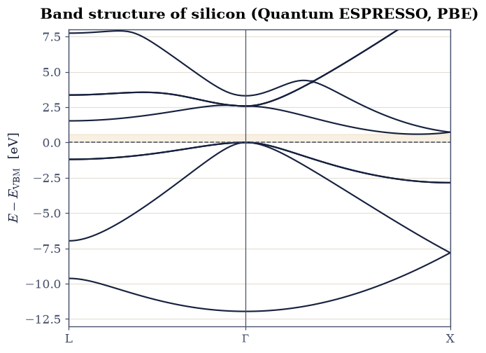
Fig. 40 Electronic band structure of silicon from the course’s Quantum ESPRESSO (PBE) calculation, along the high-symmetry path L–Γ–X, with energies referenced to the valence-band maximum (VBM, dashed). The four filled valence bands lie below the shaded gap; the conduction bands above. The VBM sits at \(\Gamma\) (amber) and the conduction-band minimum (CBM, navy) lies along \(\Gamma\)–X, so the fundamental gap is indirect.#
Validation 3 — four valence bands below the gap#
At every k-point along the path the four valence bands must lie at or below the VBM (energy \(\le 0\)), the basic structure of a filled-shell semiconductor.
✓ the four valence bands lie at or below the valence-band maximum everywhere [max valence energy relative to VBM = 0.000 eV]
True
Exercise 4 — The indirect band gap#
Read the gap off the bands. The valence-band maximum is the highest point of the fourth band; the conduction-band minimum is the lowest point of the fifth. For silicon the VBM sits at \(\Gamma\) and the CBM lies about \(0.85\) of the way from \(\Gamma\) to X, so the two are at different crystal momenta and the gap is indirect. The smallest direct gap, both extrema taken at \(\Gamma\), is far larger, which confirms the indirect character.
Part a) Find the VBM, the CBM, and their k-points.
Part b) Compute the indirect gap and the direct gap at \(\Gamma\).
VBM = 6.226 eV at Γ;  CBM = 6.810 eV at ~0.83 of Γ→X
indirect gap = 0.584 eV;  direct gap at Γ = 2.574 eV
Validation 4 — silicon’s indirect gap#
The PBE calculation must reproduce the qualitative band structure of silicon: a VBM at \(\Gamma\), a CBM away from \(\Gamma\) along \(\Gamma\)–X (so an indirect gap), and a much larger direct gap at \(\Gamma\). The indirect gap is the well-known PBE value of about \(0.6\,\)eV.
✓  the valence-band maximum is at Γ   [VBM index 45, Γ index 45]
✓  the gap is indirect: CBM lies along Γ–X, direct gap at Γ is much larger   [direct@Γ 2.57 eV vs indirect 0.58 eV; CBM at 0.83 of Γ→X]
✓  the PBE indirect gap is about 0.6 eV   [got 0.583652 vs expected 0.6 (rtol=1e-06, atol=0.1)]
True
Exercise 5 — The band-gap problem#
Silicon’s measured band gap is \(1.17\,\)eV. The PBE calculation gives barely half of that. This is not a mistake in the run or a lack of convergence: it is the band-gap problem of density-functional theory. The Kohn-Sham eigenvalues are auxiliary quantities chosen to reproduce the density, not the energies to add or remove an electron, and approximate exchange-correlation functionals miss a derivative discontinuity that the true gap contains [PL83]. The upshot is a systematic underestimate, often near a factor of two, that more expensive methods (hybrid functionals, \(GW\)) are needed to repair.
Part a) Compare the computed gap to experiment.
Part b) Confirm the underestimate.
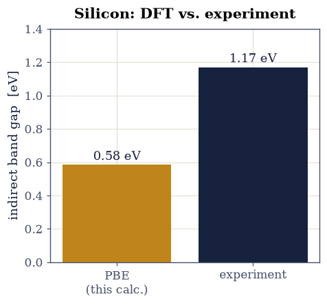
Fig. 41 The density-functional band-gap problem for silicon: the PBE Kohn-Sham gap (amber) against the experimental value of 1.17 eV (navy). PBE recovers barely half the measured gap, a systematic underestimate rooted in the missing derivative discontinuity of approximate exchange-correlation functionals, not in the convergence of the calculation.#
PBE misses the experimental gap by 0.59 eV (50% of it)
Validation 5 — DFT underestimates the gap#
The computed gap must fall well short of the experimental \(1.17\,\)eV, the signature of the Kohn-Sham band-gap problem.
✓ the PBE gap substantially underestimates the experimental value [PBE 0.58 eV vs experiment 1.17 eV (50%)]
True
Exercise 6 — The empty lattice: what comes from geometry alone#
The band structure of Exercise 3 is a result, handed over by a DFT code. It is worth asking how much of its shape needs a code at all. Strip the crystal of its potential entirely, keeping only its periodicity, and the electrons are free: their energies are \(\hbar^2k^2/2m\). Periodicity still does one thing, though. Bloch’s theorem Eq. 36 says \(\mathbf k\) and \(\mathbf k+\mathbf G\) label the same state for any reciprocal-lattice vector \(\mathbf G\), so every free-electron parabola centred on every \(\mathbf G\) gets folded back into the first Brillouin zone. What was one parabola becomes a whole family of bands:
This is the empty-lattice test, and it is the cleanest way to separate the two things a band structure contains: the part that is pure kinematics — how many bands there are, roughly how wide, where they cross — and the part that genuinely needs the potential, which is where degeneracies split and gaps open. Silicon’s Bravais lattice is face-centred cubic, so its reciprocal lattice is body-centred cubic: \(\mathbf G = (2\pi/a)(h,k,l)\) with \(h,k,l\) all even or all odd. The shortest non-zero shell is the eight \(\langle111\rangle\) vectors with \(|\mathbf G|^2 = 3\) in these units.
Part a) Build the reciprocal-lattice vectors: take all integer triples \((h,k,l)\)
in \([-2,2]\) with itertools.product and keep those whose components share a parity,
which is the fcc-reciprocal (bcc) selection rule. Evaluate Eq. 37 on
the same k-path the DFT calculation used, with the prefactor
\((\hbar^2/2m)(2\pi/a)^2\) built from scipy.constants and \(a = 5.431\) Å, then sort
the energies at each k-point with numpy.sort and keep the lowest eight.
Write this one yourself — the implementation is the lesson.
Part b) Overlay the folded free-electron bands on the DFT bands, each referenced to its own lowest state. Note what survives the stripping of the potential and what does not.
Part c) Make the comparison quantitative at \(\Gamma\). The free-electron model puts a single state at the bottom and then an eightfold degenerate level at \(3\,(\hbar^2/2m)(2\pi/a)^2\). Count how many distinct energies the DFT calculation shows among its eight lowest states at \(\Gamma\), and confirm the degeneracy is lifted. That splitting is the crystal potential doing the one job the empty lattice cannot, and silicon’s gap is what is left over when it is done.
prefactor (hbar^2/2m)(2pi/a)^2 = 5.0994 eV
free-electron shell at Gamma: 15.298 eV, 7 of the lowest 8 bands sit in it
DFT at Gamma: 4 distinct levels among 8 states -> [0.0, 11.96, 14.54, 15.26] eV
bandwidth of the lowest band, free 5.10 eV vs DFT 4.15 eV
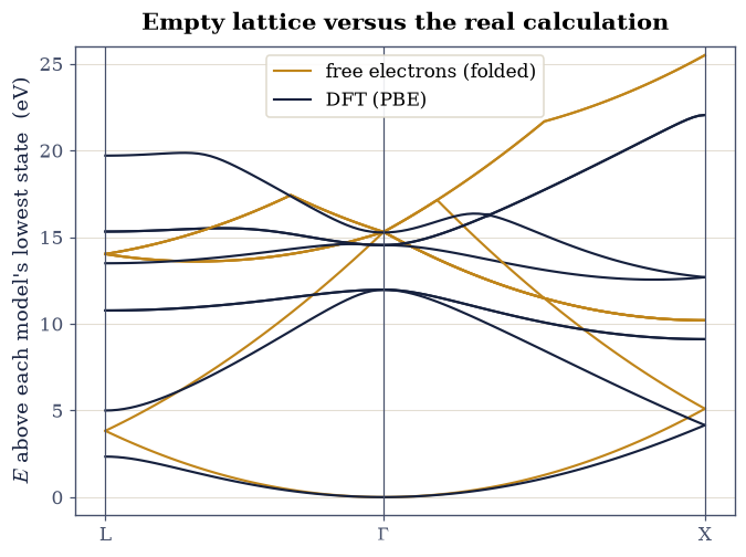
Fig. 42 The empty-lattice test for silicon along L–\(\Gamma\)–X. Amber: folded free-electron bands \(E=(\hbar^2/2m)|\mathbf k+\mathbf G|^2\) for the fcc reciprocal lattice, with no crystal potential at all. Navy: the bands from the course’s Quantum ESPRESSO calculation. Each set is referenced to its own lowest state. The number of bands, their rough widths, and the general pattern of crossings come from periodicity alone; what the potential adds is the lifting of degeneracies – most visibly the eightfold free-electron level at \(\Gamma\), which the real calculation splits into four distinct energies, opening the gap.#
Validation 6 — kinematics reproduced, degeneracy lifted#
Three checks. The free-electron shell energy at \(\Gamma\) is fixed arithmetic: \(3\,(\hbar^2/2m)(2\pi/a)^2\), and the eight \(\langle111\rangle\) vectors must all land on it. The width of the lowest band must come out comparable between the two models, since that width is kinematic rather than a property of the potential. And the DFT calculation must show that degeneracy split — which is the one thing the empty lattice provably cannot produce, and the reason silicon has a gap at all.
✓  the folded free-electron level at Gamma sits at 3 (hbar^2/2m)(2 pi/a)^2, the |G|^2 = 3 shell of the eight <111> reciprocal vectors   [got 15.2983 vs expected 15.2983 (rtol=1e-09, atol=1e-09)]
✓  the lowest band has a comparable width with and without the potential: its bandwidth is kinematics, set by the lattice rather than by the chemistry   [free 5.10 eV vs DFT 4.15 eV]
✓  and the real calculation splits the eightfold free-electron level into several distinct energies: the potential lifting that degeneracy is what opens silicon's gap   [7 free-electron states in one shell -> 4 distinct DFT levels at Gamma]
True
Exercise 7 — A tight-binding silicon beside the committed bands#
The Quantum ESPRESSO bands were read; nothing in this notebook yet computes a band structure. The classic build-it-yourself model is empirical tight binding in the sp\(^3\)s\(^\ast\) basis of Vogl, Hjalmarson and Dow [VHD83]: five orbitals per atom, nearest-neighbour couplings only, and one deliberately artificial ingredient — the excited \(s^\ast\) orbital, added not for chemistry but to stand in for the \(d\) states that push the conduction band down along \(\Delta\). Without it, no nearest-neighbour sp\(^3\) model can make silicon’s gap indirect; with it, ten parameters fitted to experiment reproduce the gap structure of an entire semiconductor family.
On the diamond lattice every atom’s four neighbours sit along \(\mathbf d_{1..4} = \tfrac a4(1,1,1),\ \tfrac a4(1,\bar1,\bar1),\ \tfrac a4(\bar1,1,\bar1),\ \tfrac a4(\bar1,\bar1,1)\), and every coupling in the \(10\times10\) Bloch Hamiltonian is one of four phase sums
with sign patterns \((++++)\), \((++--)\), \((+-+-)\), \((+--+)\) — the lattice’s geometry, Fourier transformed once and for all. The parity signs matter: \(\langle s_a|H|p_c\rangle\) and \(\langle p_a|H|s_c\rangle\) couple with opposite sign, and getting one wrong destroys the degeneracy structure at \(\Gamma\) that Part c gates.
Part a) Build \(H(\mathbf k)\) from the published silicon parameters and diagonalise it along the same L–Γ–X path as the committed QE calculation. Write this one yourself — the implementation is the lesson.
Part b) Overlay the ten tight-binding bands on the eight QE bands, both hung from their valence-band maxima.
Part c) Run the three-way comparison — tight binding, PBE, experiment — for the indirect gap, the direct gap at \(\Gamma\), and the conduction-minimum location. The moral is the point of the exercise: the empirical model lands on the experimental gaps because it was fitted to them, while the first-principles functional misses the gap for reasons no parameter can fix (ECP §8.8 computes why) — two different meanings of “predict”, and a working scientist needs both.
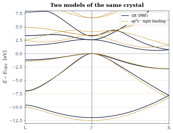
Fig. 43 The sp3s* empirical tight-binding bands of silicon (amber, dashed) overlaid on the committed Quantum ESPRESSO PBE bands (navy) along the same L–Γ–X path, both referenced to their valence-band maxima. The two calculations agree on the qualitative anatomy — a ~12 eV valence manifold, the triple degeneracy at Γ, a conduction minimum inside the Δ line — but part company exactly where their natures dictate: the tight-binding model, fitted to experiment, opens the indirect gap to the measured 1.17 eV where PBE gives 0.58, and puts the direct gap at the measured 3.4 eV where PBE gives 2.6. An empirical model knows what it was told; a first-principles functional knows why it fails.#
                 TB (fitted) PBE (ab initio)  experiment
indirect gap           1.172           0.584        1.17
direct gap (Γ)        3.430           2.574        3.40
CBM at Γ→X            0.72            0.83       ~0.85
VBM at Γ (triple, spread 1.0e-15 eV); valence width 12.5 eV (QE 12.0 eV)
Notebook summary#
We read the course’s real Quantum ESPRESSO output for silicon and turned it into the band structure along \(L\)–\(\Gamma\)–\(X\). The valence-band maximum sits at \(\Gamma\) while the conduction-band minimum lies toward \(X\), making the gap indirect, the feature that shapes silicon’s optical absorption and its role in electronics. We also met the band-gap problem: the Kohn–Sham gap from semilocal DFT underestimates the measured \(1.17\,\)eV, a known and instructive limitation of the method rather than a numerical error.
Outlook#
The other half of the handshake. The companion Elementary Computational Physics course builds this same silicon band structure from three empirical form factors with every matrix element visible (ECP §8.11) — the transparent twin of this notebook’s production DFT calculation. The two courses meet, deliberately, at the same material.
Fixing the gap. Hybrid functionals (HSE) mix in exact exchange and roughly halve the error; the \(GW\) approximation computes the true quasiparticle gap and gets silicon within a tenth of an eV (ECP §8.14 builds \(G_0W_0\) from scratch and prices its regime of validity). Both cost far more than PBE.
The density of states. Integrate the bands over the whole Brillouin zone (not just the path) to get \(g(E)\), which is what optical and transport measurements actually probe.
Other crystals. The course also ran silicon carbide and a graphene nanoribbon; rerunning this analysis on them shows a wider gap (SiC) and the one-dimensional bands of the ribbon.
Effective masses. The curvature of the bands at the VBM and CBM, \(1/m^\* = \hbar^{-2}\,d^2E/dk^2\), sets the mobility of electrons and holes; fit a parabola near each extremum to extract it.
References#
Neil W. Ashcroft and N. David Mermin. Solid State Physics. Holt, Rinehart and Winston, 1976.
Paolo Giannozzi and others. Quantum espresso: a modular and open-source software project for quantum simulations of materials. Journal of Physics: Condensed Matter, 21(39):395502, 2009. doi:10.1088/0953-8984/21/39/395502.
Richard M. Martin. Electronic Structure: Basic Theory and Practical Methods. Cambridge University Press, 2 edition, 2020.
John P. Perdew, Kieron Burke, and Matthias Ernzerhof. Generalized gradient approximation made simple. Physical Review Letters, 77(18):3865–3868, 1996. doi:10.1103/PhysRevLett.77.3865.
John P. Perdew and Mel Levy. Physical content of the exact kohn-sham orbital energies: band gaps and derivative discontinuities. Physical Review Letters, 51(20):1884–1887, 1983. doi:10.1103/PhysRevLett.51.1884.
P. Vogl, Harold P. Hjalmarson, and John D. Dow. A semi-empirical tight-binding theory of the electronic structure of semiconductors. Journal of Physics and Chemistry of Solids, 44(5):365–378, 1983. doi:10.1016/0022-3697(83)90064-1.